GPU architecture
The architecture and design mode of GPU is introduced with examples, in comparison with the CPU architecture.
All the pics and contents are not original. The contents of the whole series are mainly collected from:
| Outline |
|---|
| Why need GPU |
| 3 design ideas to speedup |
| examples |
| GPU memory design |
| Terms | |
|---|---|
| FLOPS | Floating-point OPerations per Second |
| GFLOPS | One billion (10^9) FLOPS |
| TFLOPS | 1000 GFLOPS |
Why GPU
Application Driven, many applications requires computation.
GPU Structure
A GPU is a heterogeneous chip multi-processor (highly tuned for graphics).
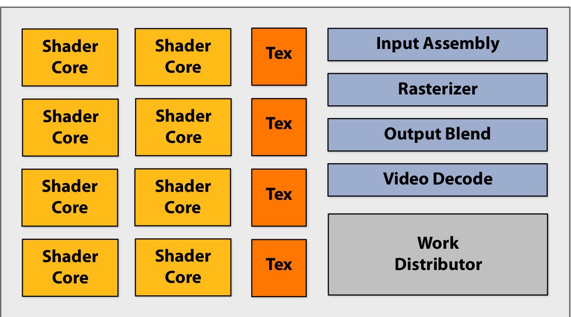
Shader Core --> ALU( Arithmetic logic unit ), basic computation unit. Before its designed specifically for image rendering, now it is able to perform general arithmetic operations.
Execute shader
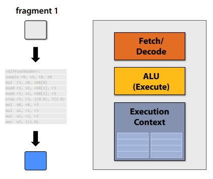
Compared with the CPU types cores, there is no cache or extra OoO, branch predictor and memory pre-fetcher, which are not related to regulated instruction processing.
3 design idea to speedup
Idea 1: multi “slimmed down cores” in parallel
- removing components that help a singe instruction stream run fast
- multi cores, multi fragments in parallel
- instruction stream sharing, multi fragments need to share one instruction stream. Otherwise a complicated control system is needed.
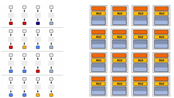
Idea 2: multi ALUs in one core
Amortize cost/complexity of managing an instruction stream across many ALUs. Design multiple ALUs in one core - SIMD. Vector operations in one core.
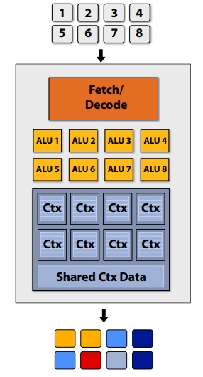
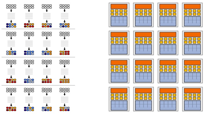
For the overall design for now, there are 16 streams for 128 fragments, technically, the 16 streams can be same or different. The 8 ALUs in one core share the same stream.
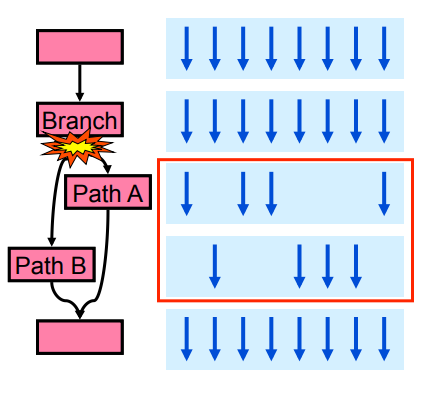
Branch divergence
With multiple ALUs sharing one stream, the parallel performance will deteriorate dealing with branches such as below:
if (x > 0)
{
    y = pow(x, exp);
    y *= K3;
    ref = y * K3;
}
else
{
    y = 0;
    ref = K3;
}
When execute this thread, different ALU will get different true or flase. However, all the ALU's must execute the same path. As a result, as the image below shows, the ALUs going to Path B have to do useless work together with the ALUs who are doing the useful work. With a such branch, and 8-thread core, the performance can be as low as 1/8 peak performance.
Just to clarify here, not all the SIMD process need explicit SIMD instruction. There are two options in total:
- explicit vectorized instructions, SSE for example
- implicit sharing managed by hardware, provide scalar instructions and the hardware share them.
- one scalar instruction is shared by multi-threads
- NVIDIA for example
Stalls
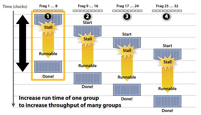
Stalls occur when a core cannot run the next instruction because of a dependency on a previous operation. Wait until ready. In order to deal with stalls, we have a third idea.
Idea 3 Switch between different fragments to hide latency.
Interleave processing of many fragments on a single core to avoid stalls caused by high latency operations.
To maximise latency hiding, the context storage space is split into multiple components as demonstrated:
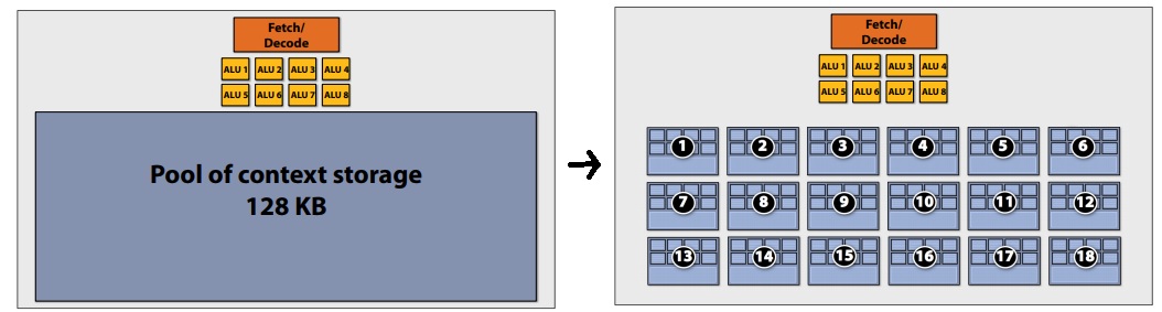
Actually there are 3 level of context storage division:
- 18 small contexts, maximal latency hiding, fragments are small
- 12 medium contexts,
- 4 large contexts, more work for each fragments, but low latency hiding ability
Just to clarify here, interleaving between contexts can be managed by hardware (HW) or software (SW) or both
- NIVIDIA / ATI Radeon GPUs (HW only)
- HW schedules / manages all contexts (lots of them)
- Special on-chip storage hods fragment states
- Intel Larrabee (Both)
- HW manages 4 x86 (big) contexts at fine granularity
- SW scheduling interleaves many groups of fragments on each HW context
- L1 - L2 cache holds fragment state (as determined by SW)
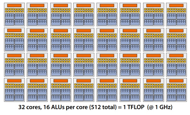
Overall design
Our overall design has the following specifications:
- 32 cores
- 16 mul-add ALUs per core (512 total)
- 32 simultaneous instruction streams
- 64 concurrent (but interleaved) instruction streams
- 512 concurrent fragments = 1 TFLOPs (@ 1GHz)
Real designs
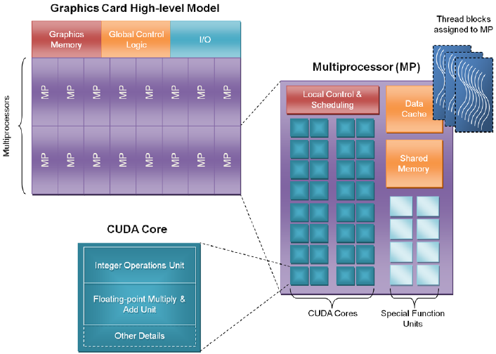
MP = SM = core
CUDA core = ALU
CUDA thread = fragment
The SM is the heart of NVIDIA’s unified GPU architecture. Most of the key hardware units for graphics processing reside in the SM. The SM’s CUDA cores perform pixel/vertex/geometry shading and physics/compute calculations. Texture units perform texture filtering and load/store units fetch and save data to memory. Special Function Units (SFUs) handle transcendental and graphics interpolation instructions. Finally, the PolyMorph Engine handles vertex fetch, tessellation, viewport transform, attribute setup, and stream output.
NVIDIA GeForce GTX 480 (Fermi)
Specifics:
- NVIDIA-speak:
- 480 stream processors ("CUDA cores")
- "SIMT" execution
- Generic speak
- 16 (SM) cores
- 2 groups of 16 SIMD functional unites per core
Some notes:
1 SM contains 32 CUDA cores
2 warps are selected each clock (decode, fetch, then execute 2 warps in parallel)
Up to 48 warps are interleaved, totally 23000 CUDA threads
NVIDIA GeForce GTX 680 (kepler)
 architecture.png)
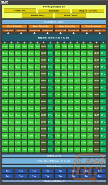
| GPU | GF110 (Fermi) | GK104 (Kepler) |
|---|---|---|
| Per GPU: | ||
| SM / SMXs | 16 | 8 |
| Per SM unit counts : | ||
| CUDA Cores | 32 | 192 |
| Special Function (Units SFU) | 4 | 32 |
| load/store units (LD/ST) | 16 | 32 |
| Texture units (Tex) | 4 | 16 |
| Polymorph | 1 | 1 |
| Warp schedulers | 2 | 4 |
SMX means a powerful SM
NVIDIA GK110
SMX: 192 single-precision CUDA cores, 64 double-precision units, 32 special function units (SFU), and 32 load/store units (LD/ST).
GPU memory design
The importance of bandwidth
GPU memory design
Compare with CPU-Style core:
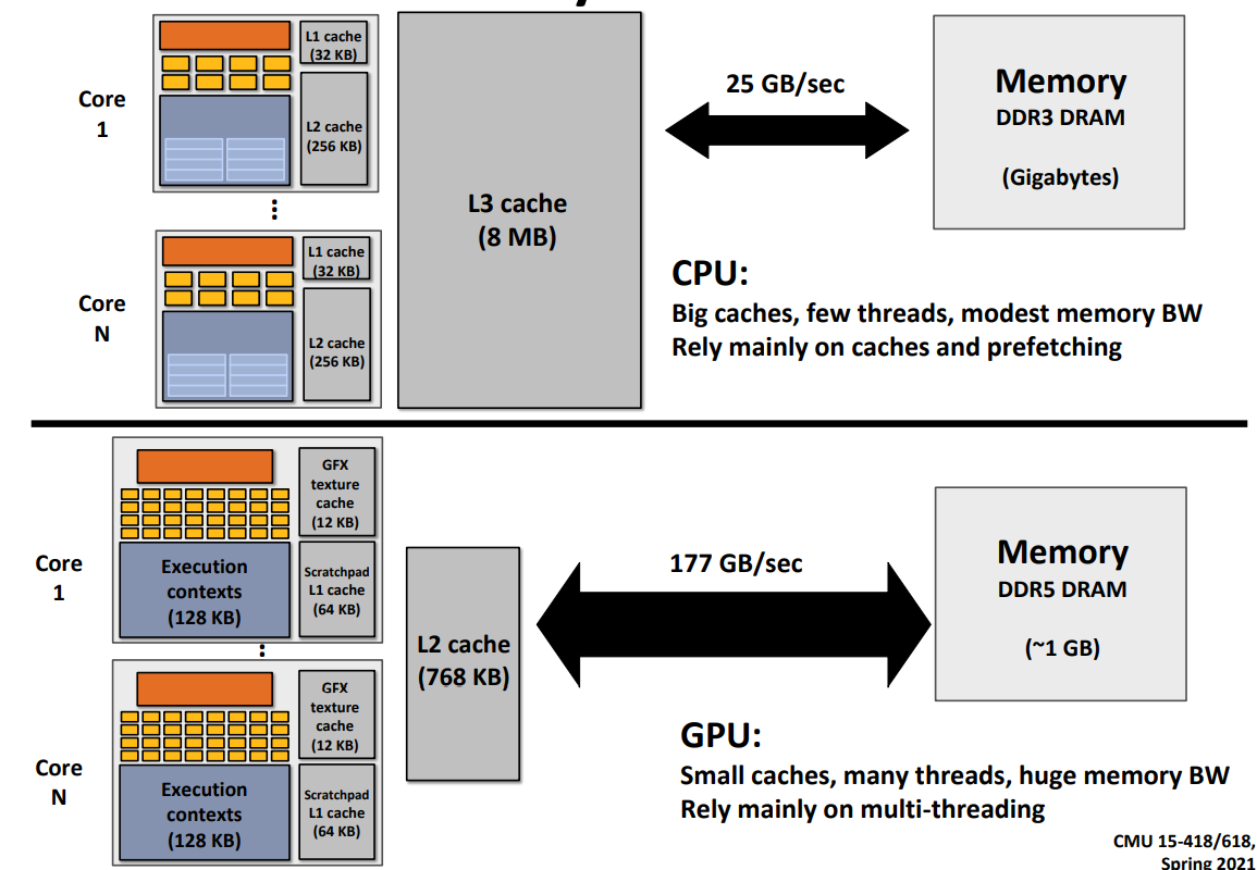
The cache area in CPU is huge, and is is divided into 3 levels, L1, L2 and L3 caches. Inside the caches, the latency (length of stalls) is low and the bandwidth is big. Yet the bandwidth is low to the outside memory, as low as 12GB/s. The CPU cores run efficiently when data is resident in caches.
In GPU (throughput style), no large cache hierarchy exists. As a result a high bandwidth to the memory is required, as high as 150GB/s.
Although the GPU memory bandwidth is high, it is only 6 times to the CPU. It is still not enough compared with the compute performance of GPU(over 10 times to the CPU).
Bandwidth thought experiment
Task: element-wise multiply two long vectors A and B then plus C of the same length, save the result to vector D. here are the steps:
- Load input
A[i] - Load input
B[i] - load input
C[i] - Compute
A[i]*B[i]+C[i] - Store result into
D[i]
There are 4 memory operations (16 bytes) for every MUL-ADD operation.
Radeon HD 5870 can do 1600 MUL-ADDs per clock
Need ~20TB/s of bandwidth to keep ALUs busy
It is less than 1% efficiency, but still 6x faster than CPU, because of the bandwidth limit.
Bandwidth limited
If processors request data at too high a rate, the memory system cannot keep up. No amount of latency hiding helps this. Overcoming bandwidth limits are a common challenge for GPU-compute application developers.
In practice, when working on a large nerual networks, say BERT or GPT-2. The actual FLOPS will not reach the thoretical FLOPS calculated by the number of the matrix operations. The main reason are the activation layers and operation of SGD. They are compuational light yet memory heavy operations. The bandwidth will deter the calculation on these steps.
Reducing bandwidth requirments
- Request data less often (do more math instead), "arithmetic intensity"
- Fetch data from memory less oftern (share/reuse data across fagments)
- on-chip communication or storage
Examples
- Texture caches
- Capture reuse across fragments, not temporal reuse within a single shader program
- OpenCL "local memory", CUDA shared memory
Note: OpenCL is an open standards version of CUDA - CUDA only runs on NVIDIA GPUs - OpenCL runs on CPUs and GPUs from many vendors - Almost everything about CUDA also holds for OpenCL - CUDA is better documented, thus I find it preferable to teach with.
Mordern GPU memory hierarchy
Shown on pictures above, the GPU possesses:
On-chip storage takes load off memory system
Many developers calling for more cache-like storage
(particularly GPU-compute applications)
A good GPU task
- Many many independent tasks
- exploiting massive ALUs
- many fragments switch to hide latency
- Shared instructions
- suitable for SIMD processes
- arithmitic intense task
- suitable commination and computation proportion
- not limited by share-load bandwidth